
Firstly, the conclusion is drawn: Generally, we set the PCB below the vertical plane of the isolated driver chip as a prohibited wiring layer, neither passing any signals nor placing various components, as shown in Figure 1. Then we will discuss why wiring cannot be done, and finally introduce exceptional applications.


Why is wiring not recommended below the chip?
Because it will affect normal signal transmission! Since you are using an electrically isolated driver chip, you definitely hope that there is no tie between the primary and secondary sides, and the power supply of the two is independent and meets the application isolation requirements. Therefore, there are generally no electrical connection wires on both sides. So, can the reference point for the bridge be extended to the original side of the chip? The conclusion is that it is not necessary, after all, spatial closeness requires coupling effects. The usually changing voltage will inject distributed current through the coupling capacitor; The changing current will cause induced electromotive force. Especially for high-power switching devices with high frequency and high voltage, the dv/dt at the midpoint of the upper and lower bridges is often very large. If the source or emitter potential of the upper bridge is covered with copper on a large area or even on the original side, it is very dangerous. It may introduce various sizes of distributed currents, exceeding the limit value can cause logic signal disorder and even chip damage. Even if there is no copper layer coupling relationship on both sides of the chip, the driving chip still has a tolerance to dv/dt, which is the CMTI value in the specification. It marks the maximum dv/dt that the device can withstand under normal use. Infineon’s driving products are at the leading level in the industry, with some models reaching up to 300V/ns, which can be applied to high-speed switching devices such as SiC and GaN.
Ground signal without voltage change
Can it be laid under the driver chip?
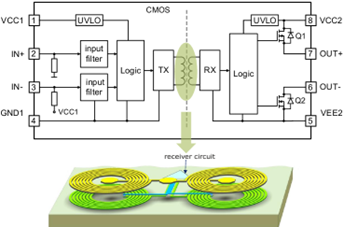
Although the ground potential of the lower bridge is relatively stable, if it is the main power ground, there will be alternating current passing through, which may affect the signal transmission of the non magnetic core transformer inside the Infineon isolation drive. As mentioned earlier, Infineon’s isolation drive products have strong resistance to dv/dt, which is a benefit of the electrical isolation technology based on magnetic coupling (Figure 2). The switch commands and other signals between the input and output sides are transmitted in the form of current changes. And there are two sets of reverse wound wire coils on the signal transmission side and the reception side, as shown in Figure 2. When there is strong external current interference, the generated interference current is of equal magnitude and opposite direction, which can cancel each other out. In addition, based on Infineon’s years of experience in chip logic design, the product will also have various filtering and shaping circuits inside to suppress this interference. Furthermore, the impact of current changes is not only related to the size of the interference source itself, but also closely related to factors such as relative distance and position direction. This provides feasible solutions for vertical structures that appear to have strong interference. This is the exception in the next section.

The situation where the driver board is directly installed on the module
Is there a situation where there is a high current under the driver chip in practical applications? Yes, such as Figure 3. The entire driver board is welded above the module, and there must be current flowing through the module, which is very likely to appear directly below the driver chip. However, in reality, it does not interfere with the normal operation of the driver during operation, as the changing current is sufficiently distant from the coreless transformer inside the chip. Based on usage experience, there is generally no problem with a distance of more than 5mm.

summary
It is best not to send any signals directly below the driver of the power switching device. If it is necessary to leave, then various verification work must be done to ensure that the entire system can work normally and there will be no wave loss, waveform distortion, or even accidental triggering of the waveform. For example, under different load powers, temperatures, overcurrent or even short-circuit conditions, the chip will not be disturbed.